Close
![Popup Image]()
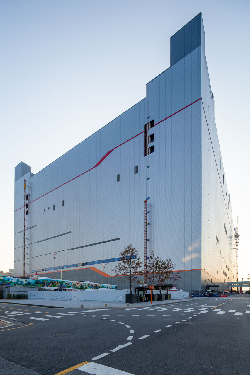
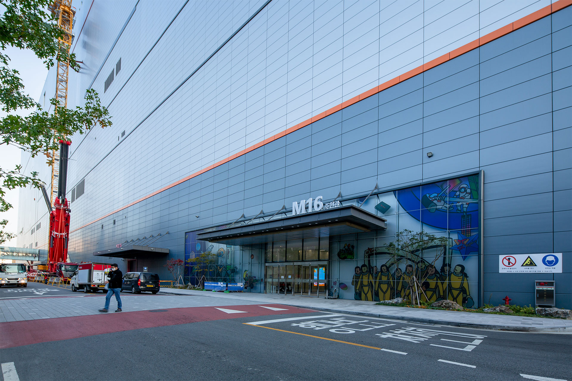
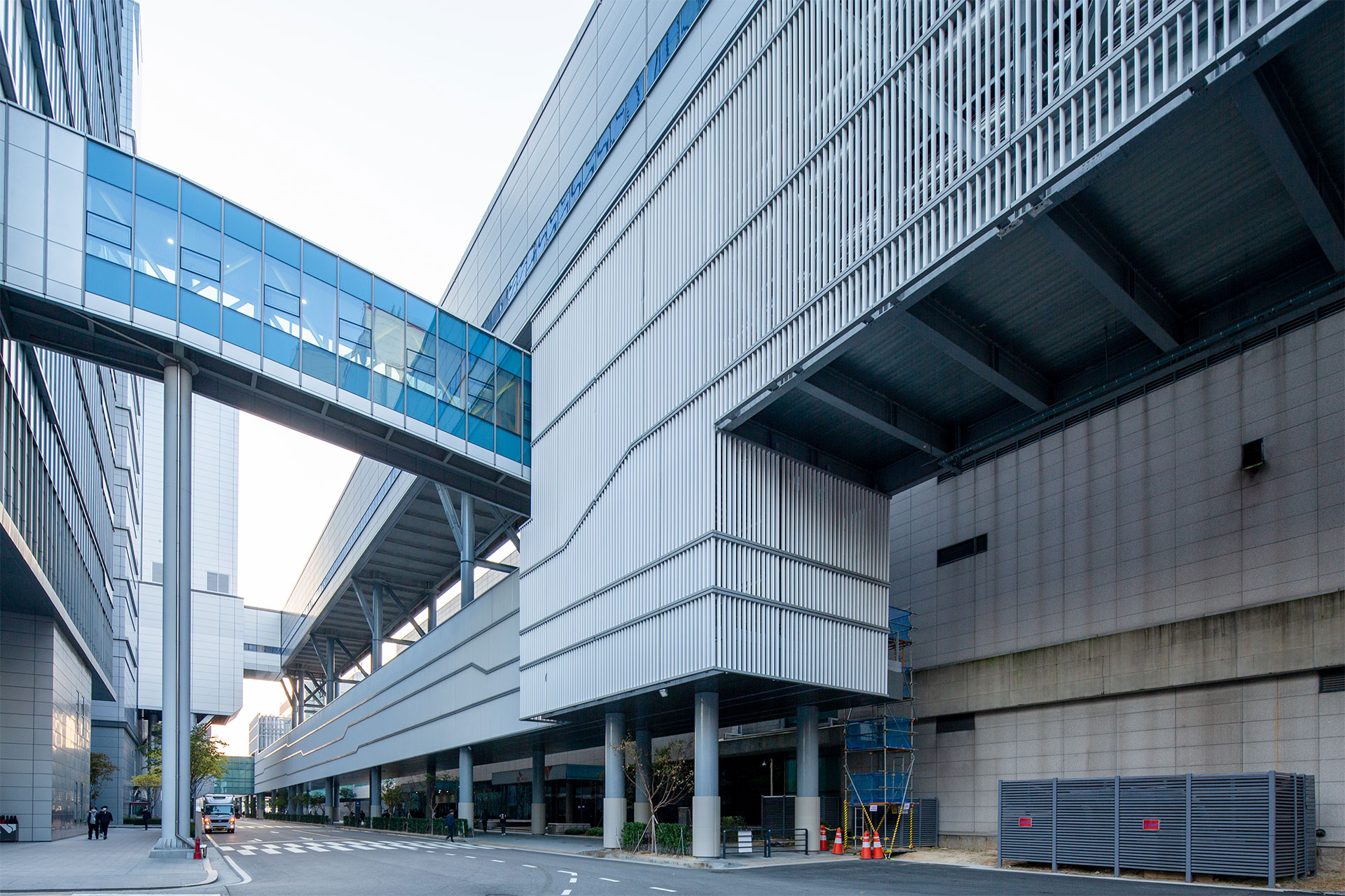
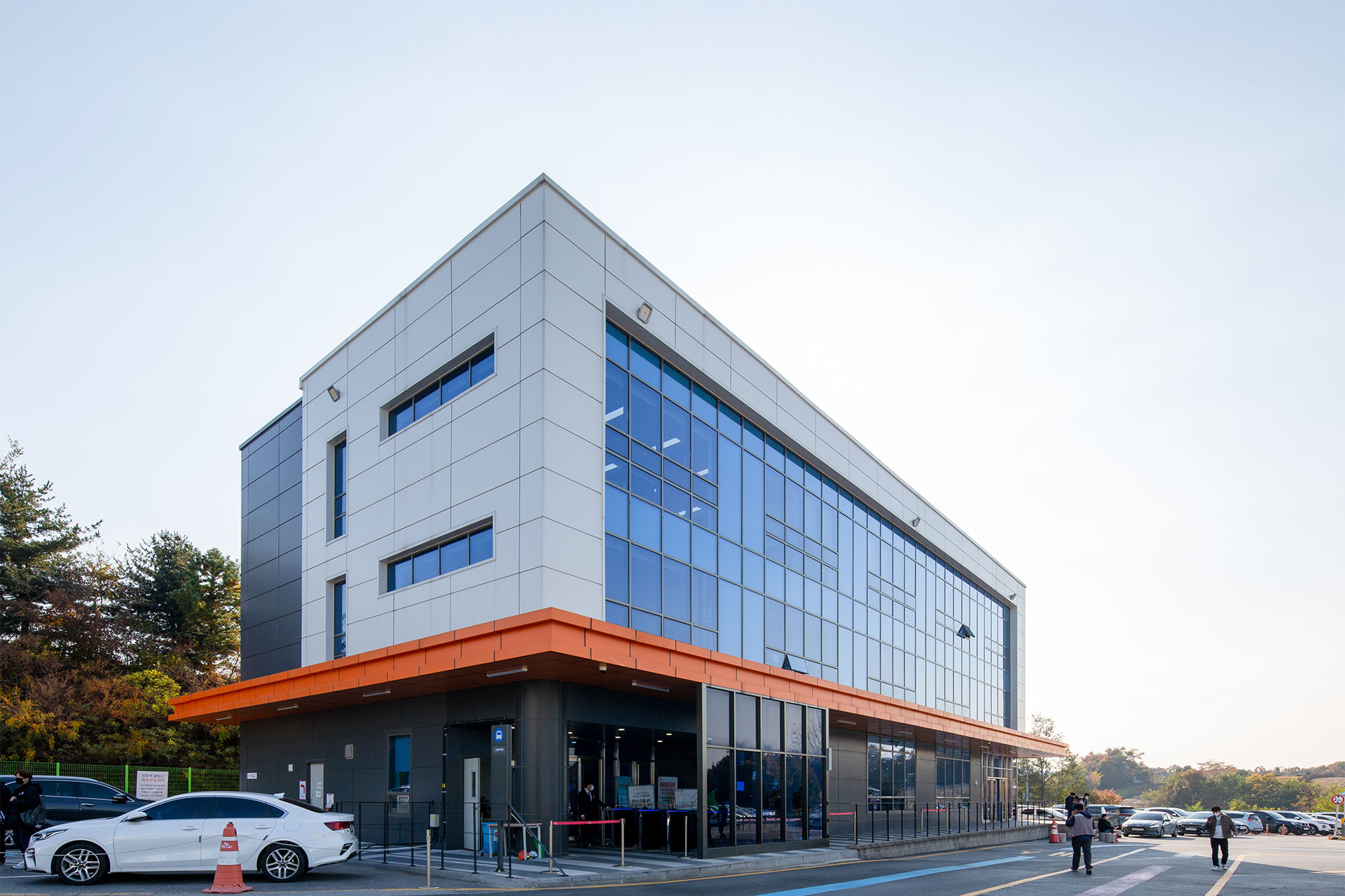
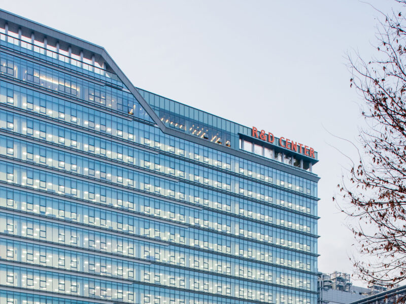
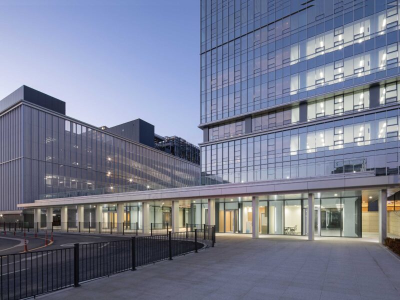
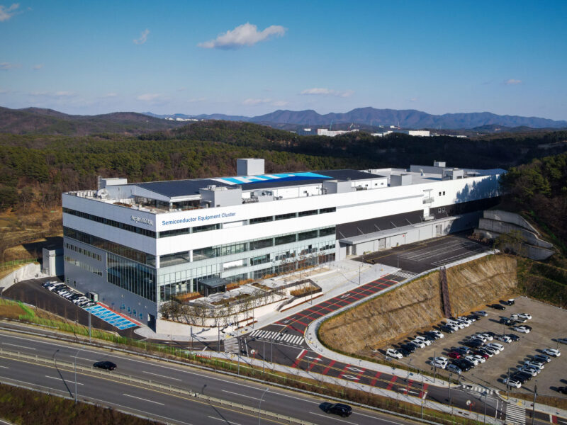
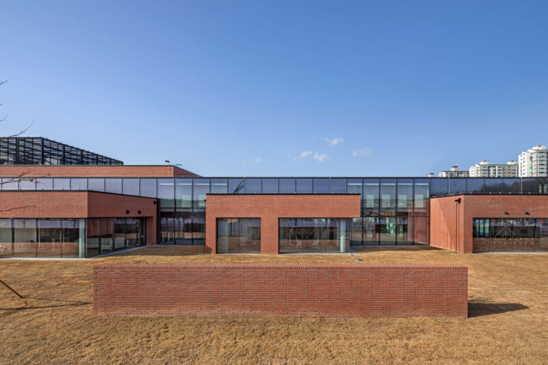
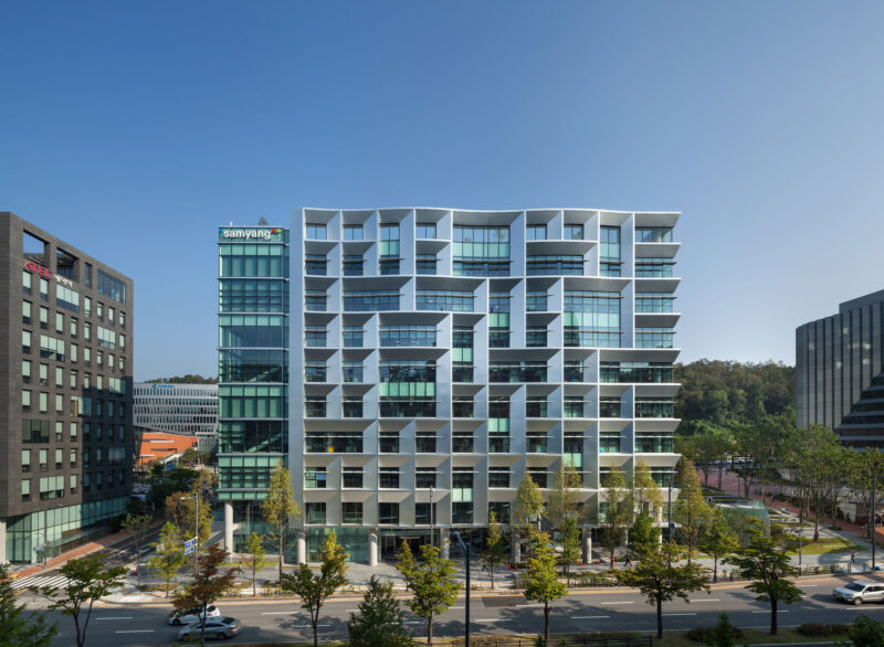
The SK Hynix M16 is a project to construct the largest semiconductor (D-RAM) production building and auxiliary facilities in Korea on the site of a demolished existing line and idle land. Junglim Architecture was responsible for the architectural design of the main FAB building and auxiliary buildings, participating from the planning stage through to completion.
The semiconductor line construction followed a typical fast-track approach, with BIM applied throughout the main FAB building’s design process. Developed as an expandable facility, the Icheon campus, now saturated, was given a campus concept, with design and site work focused on ensuring smooth utility (UT) flows between facilities.
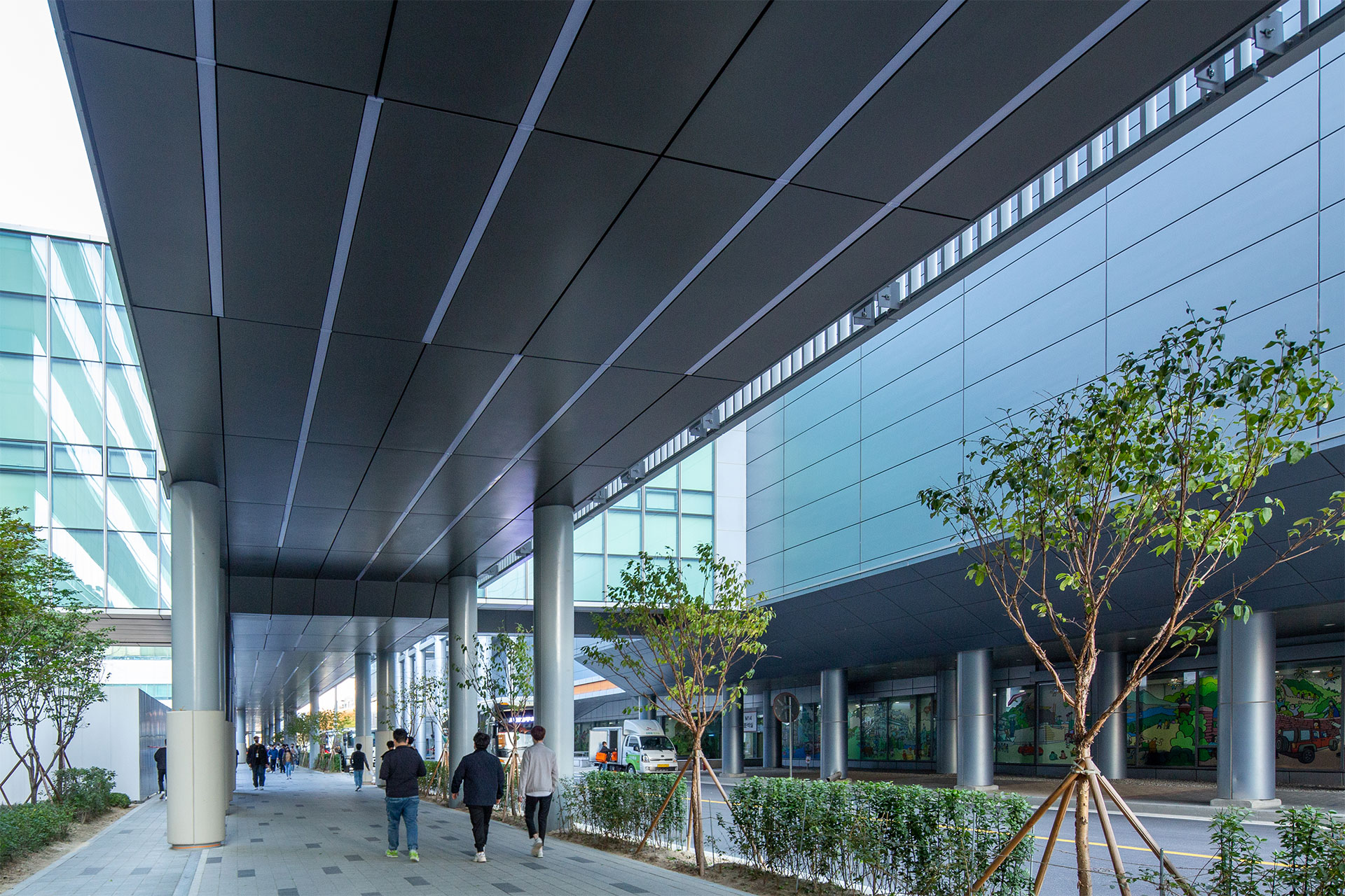
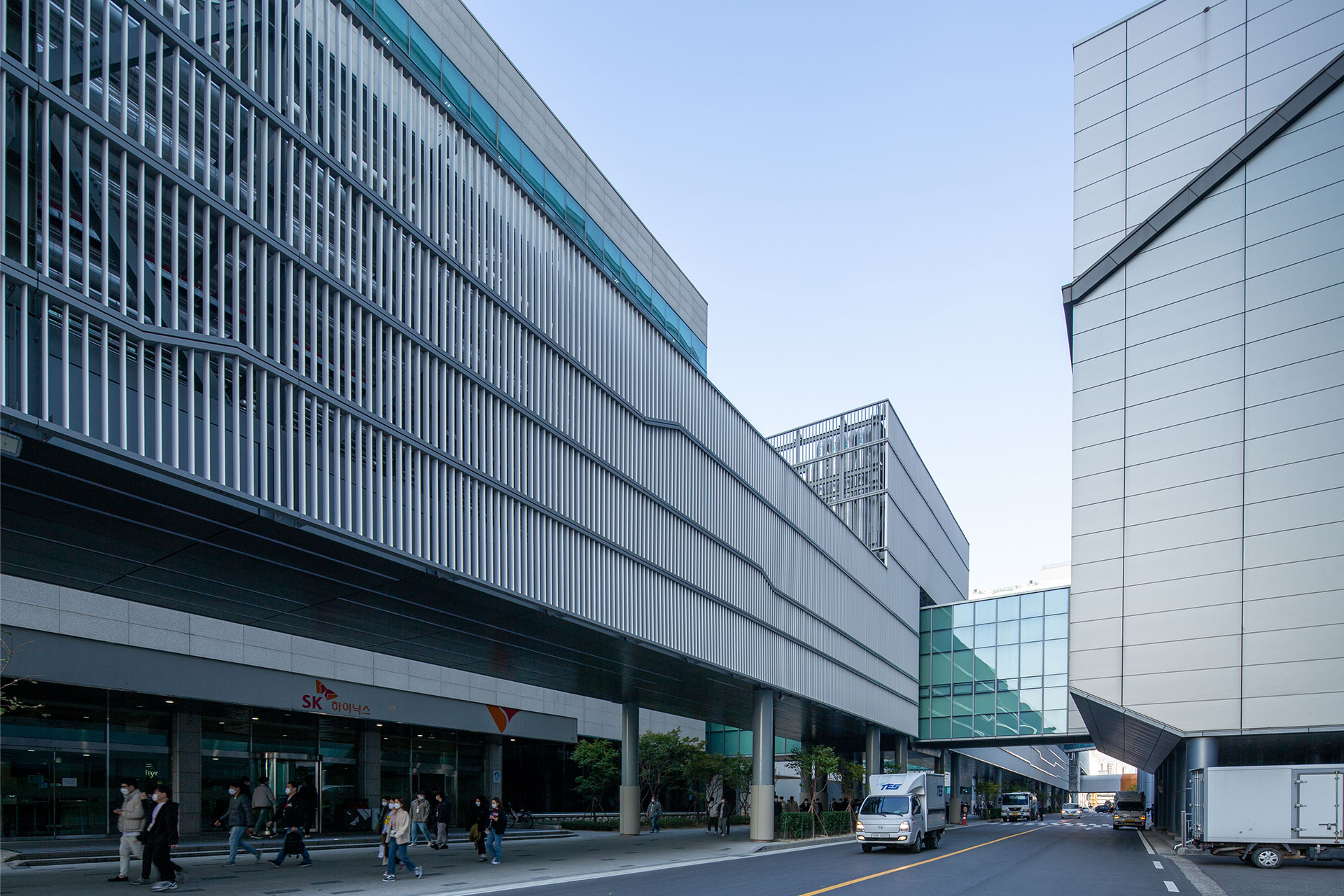
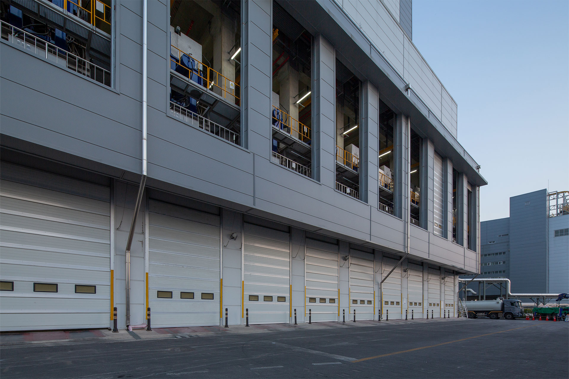
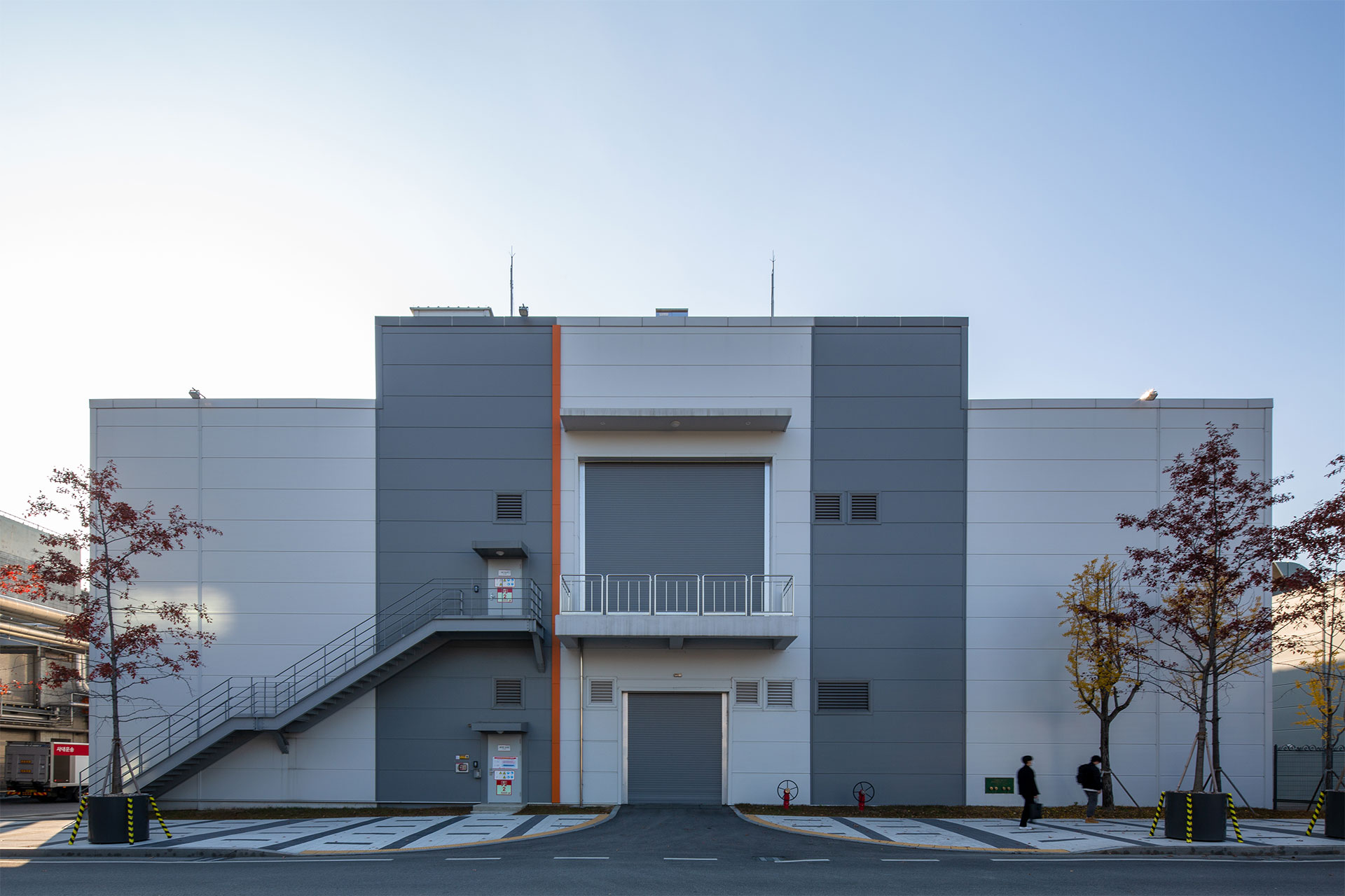
The lower floors of the FAB building house the next-generation production equipment called EUV (Extreme Ultraviolet), testing, and development lines, with upper and lower FABs combined to pioneer the world’s first “3-layer FAB.” The core of the auxiliary buildings, the Central Utility Building (CUB), was planned to function as a hub facilitating the organic space arrangement of five different facilities and the smooth supply and return of utilities. Facade, interior, and landscaping designs emphasized a modern industrial park image to create a vibrant Icheon campus for Hynix staff and partner companies.
-
Status
Completed
-
Client
SK Hynix
-
Program
Industrial, Office
-
Design Year
2018
-
Completion Year
2023
-
Location
Icheon-si, Gyeonggi-do
-
Site area
798,697.00m2
-
Gross Floor Area
1,680,194.00m2
-
Building Area
387,651.00m2
-
Number of Levels
B1, 12F
-
Design
The SK Hynix M16 is a project to construct the largest semiconductor (D-RAM) production building and auxiliary facilities in Korea on the site of a demolished existing line and idle land. Junglim Architecture was responsible for the architectural design of the main FAB building and auxiliary buildings, participating from the planning stage through to completion.
The semiconductor line construction followed a typical fast-track approach, with BIM applied throughout the main FAB building’s design process. Developed as an expandable facility, the Icheon campus, now saturated, was given a campus concept, with design and site work focused on ensuring smooth utility (UT) flows between facilities.
The lower floors of the FAB building house the next-generation production equipment called EUV (Extreme Ultraviolet), testing, and development lines, with upper and lower FABs combined to pioneer the world’s first “3-layer FAB.” The core of the auxiliary buildings, the Central Utility Building (CUB), was planned to function as a hub facilitating the organic space arrangement of five different facilities and the smooth supply and return of utilities. Facade, interior, and landscaping designs emphasized a modern industrial park image to create a vibrant Icheon campus for Hynix staff and partner companies.